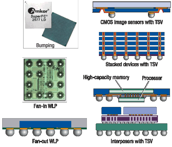
Scaling Bump Pitches In Advanced Packaging
By A Mystery Man Writer
Description
Higher density of interconnects will enable faster movement of data, but there's more than one way to achieve that.
Hybrid Bonding Process Flow - Advanced Packaging Part 5
RDL: an integral part of today's advanced packaging technologies
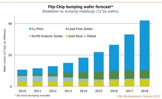
Cu pillar and micro-bumping reinvigorate Flip-Chips - News

IBM Garage: A Cloud Pak Show Case – Solution Component, 47% OFF

Terry Turner posted on LinkedIn
Fabrication process of fine pitch Cu/Sn micro-bumps using EEB
Advanced Packaging Part 1 – Pad Limited Designs, Breakdown Of Economic Semiconductor Scaling, Heterogeneous Compute, and Chiplets

Next Steps For Panel-Level Packaging

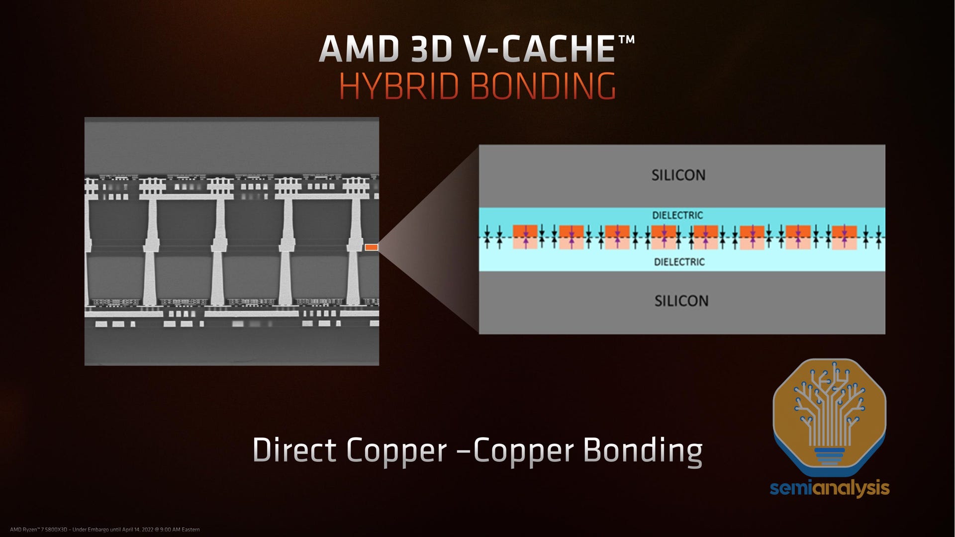
Marco Mezger on LinkedIn: #interconnects #ic #data #data #technologies #copper…

advanced packaging « PRADEEP's TECHPOINTS
Electronics, Free Full-Text

Printing Solder Paste_ Electroforming Process for Stencil Manufacturing

Puzzles are the analog way people are curbing their stay-at-home, puzzles
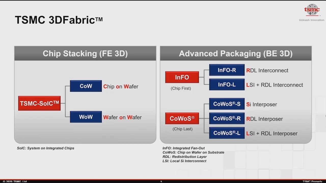
3DFabric: The Home for TSMC's 2.5D and 3D Stacking Roadmap
Random Photos
from
per adult (price varies by group size)