What is a Pad in PCB Design and Development
By A Mystery Man Writer
Description
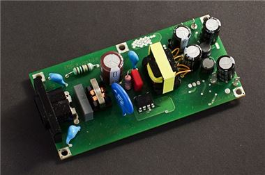
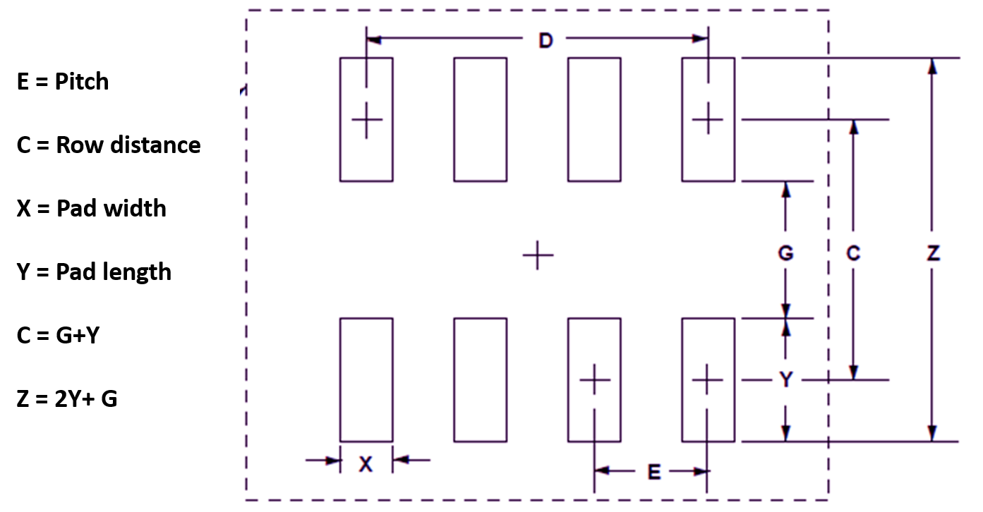
A pad is critical to PCB design as it serves as the designated surface area for electrical contact between the component and the board.
Component Placement in PCB Design & Assembly

What is Thermal Relief in PCB during the PCB Manufacturing Process
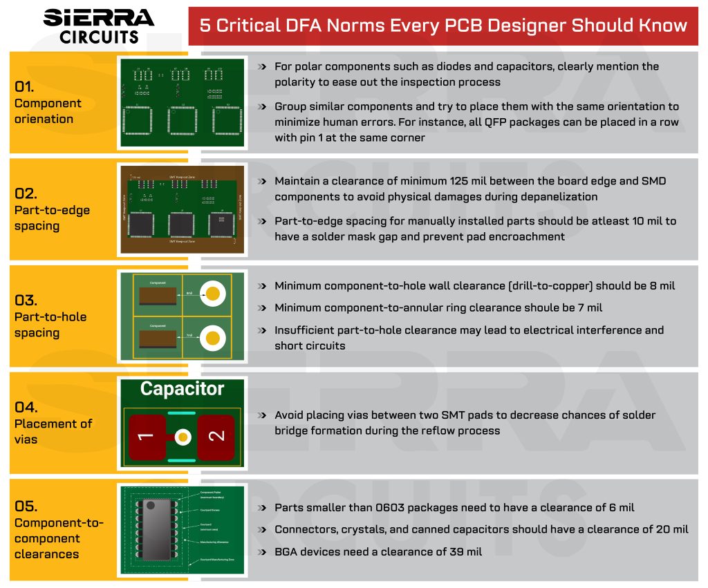
14 Tips For PCB Design For Assembly

PCB Fab Express on LinkedIn: RAPID PROTOTYPE SERVICE
PCB Basic Knowledge_84
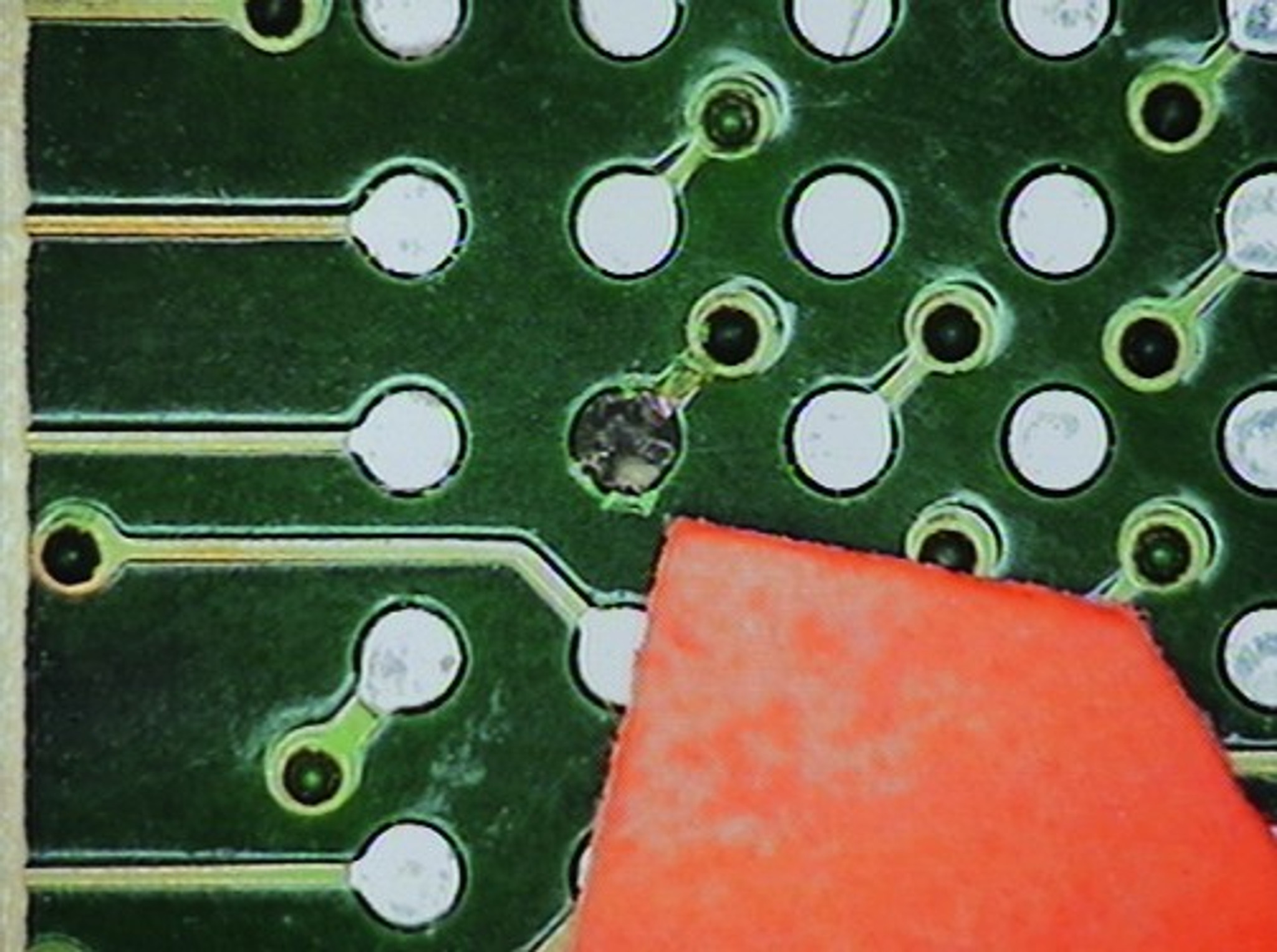
How To Repair Damaged /Missing PCB Pads INVISIBLE Fix, 45% OFF
PCB Basic Knowledge_100

PCB Fab Express on LinkedIn: RAPID PROTOTYPE SERVICE
What is a Pad in PCB Design and Development
PCB Basic Knowledge_84

What is a Pad in PCB Design and Development
from
per adult (price varies by group size)