Latest advance on seamless metal-semiconductor contact with
By A Mystery Man Writer
Description

The Intricacies of Lead Frames in the Semiconductor Industry

Metal-Semiconductors Contacts - Engineering LibreTexts

Alleviation of Schottky barrier heights at TMDs/metal interfaces with a tunneling layer of semiconducting InSe nanoflake - ScienceDirect
PDF) Proposal for all-graphene monolithic logic circuits

ELNES at the 1T /2H-MoTe 2 boundary. (a) A HAADF image showing the
DMP Factory 500 Solution - Metal 3D Printer
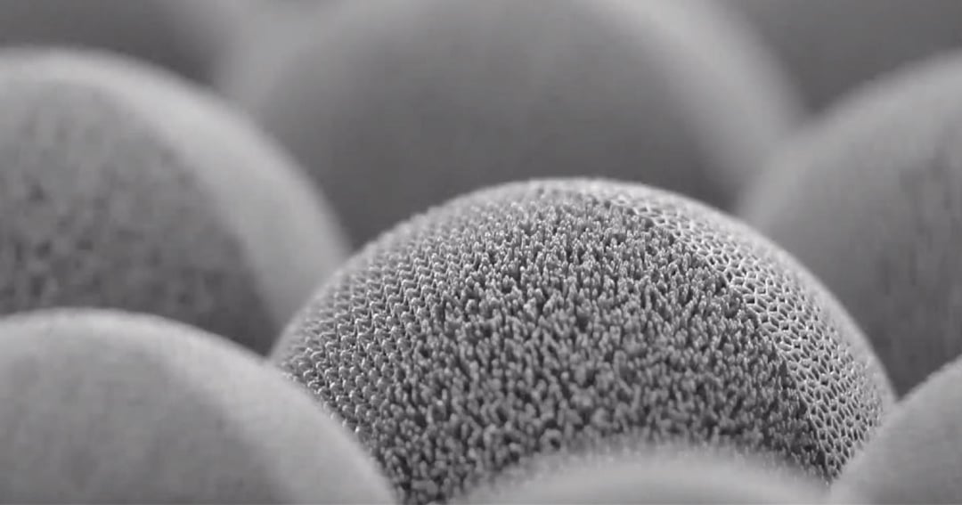
High-Performance Ceramic End Effectors - Top Seiko Co,. Ltd.

ECI Technology Wet Chemistry Process Controls Enabling Semiconductor, Advanced Packaging and PCBs by ECI-Technology - Issuu

Development of Schottky barrier field-effect transistors (SB-MOSFET) with ultra-low thermal budget

Development of Schottky barrier field-effect transistors (SB-MOSFET) with ultra-low thermal budget

Single step ohmic contact for heavily doped n-type silicon - ScienceDirect

Zonghoon LeeUNIST News Center
from
per adult (price varies by group size)