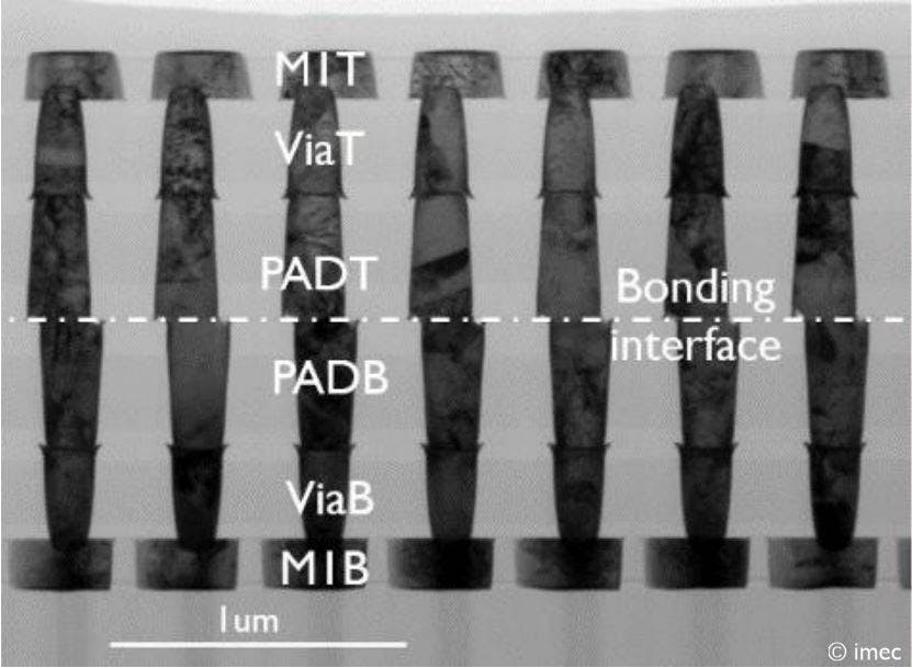
Details of test chip designs: pad pitch, layout, materials, and opening.
By A Mystery Man Writer
Description
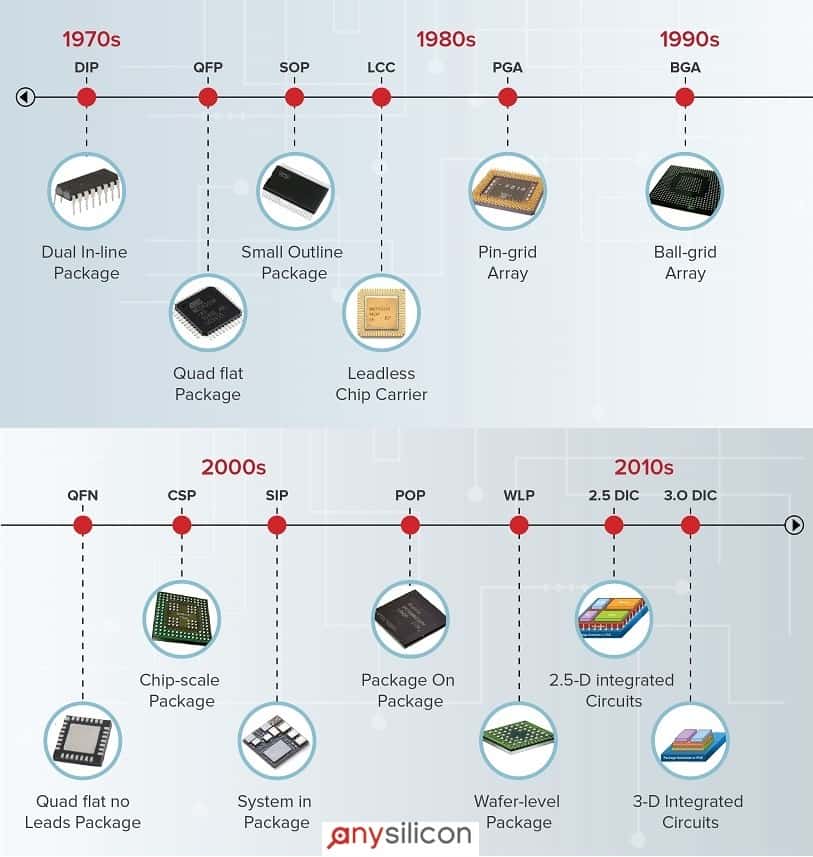
The Ultimate Guide to Semiconductor Packaging - AnySilicon

Micromachines, Free Full-Text

Hybrid Bonding Process Flow - Advanced Packaging Part 5
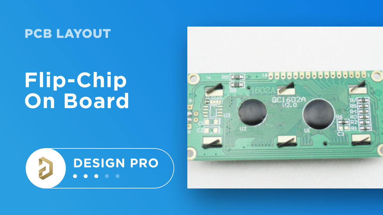
PCB Design Rules for Chip-on-Board Layout

Details of test chip designs: pad pitch, layout, materials, and opening.
Electronics, Free Full-Text
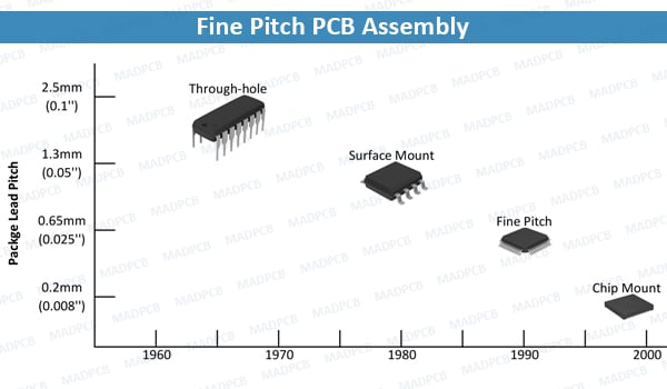
Fine Pitch Technology (FPT): PCB Board Assembly
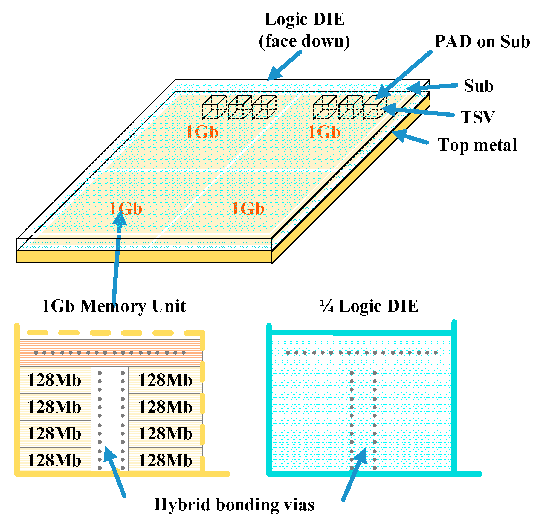
Wafer-to-wafer hybrid bonding

Taking on the 0.3 mm ultra-fine pitch device challenge in PCB design

Challenges and recent prospectives of 3D heterogeneous integration

Automated fabrication of hybrid printed electronic circuits
from
per adult (price varies by group size)